
PROVIDES THE BEST SOLUTIONS
FOR A WIDE RANGE OF CUSTOMER NEEDS
While focusing on our primary business of manufacturing materials used in the production of semiconductors, we have been actively expanding business domains into semiconductor package manufacturing, LCD manufacturing, 3D packaging and image sensor / MEMS manufacturing, based on state-of-the-art technologies and their enhanced applications.
We are also exploring new business areas such as solar panels and Nano imprinting through R&D activities with a new perspective, not merely being based on applications of existing technologies. Going forward, we plan to create functional materials by responding swiftly to market trends, as well as seeking the maximum use of micro processing technology to develop new products. In this way, we will continue actively expanding our business domains in various industries.
Semiconductor Manufacturing Field Solutions
Semiconductor companies build devices that are used for a wide range of products including information terminals such as smartphones and tablets, home electrical appliances, PC’s, automobiles and precision machinery. These devices are also used for the most advanced technologies, such as servers and super computers. Along with the increasing flexibility of applications, a wide variety of semiconductor devices have been developed.
In order to respond to wider and diversifying market needs, we have released new types of photoresists such as g-line / i-line photoresists for submicron level processing, and KrF / ArF photoresists for nanometer level processing. We are also actively working to develop photoresists for ArF immersion as well as new products for EUV / electron beam which many consider to be the next-generation light sources.
At the same time, we are working to develop a state-of-the-art photoresist based on innovative ideas and careful verifications through various research activities. The new photoresist will enable ultra-micro processing technology targeting the 10 nanometer scale. In addition to the above mentioned products, we also offer developing solutions, stripping solutions, thinners, and other high purity chemicals. We support the semiconductor manufacturing industry with our comprehensive strength of combining advanced processing technologies and various types of processing equipment.
TOK America is able to offer the semiconductor industry i-line photoresists which are made in the U.S., as well as developer solutions (NMD-W and NMD-3 2.38%), and post etch stripping solutions. Our U.S. team is ready to support your needs. For the entire lineup of resists, we are happy to supply you with our high quality products manufactured in both our US and Japanese factories.
Semiconductor Packaging Manufacturing Technology
In addition to being equipped with highly sophisticated functions, mobile devices are rapidly becoming lighter, thinner and more compact in a pace much faster than we could have imagined. Packaging and MEMS manufacturing technologies play an extremely important role for such advancement.
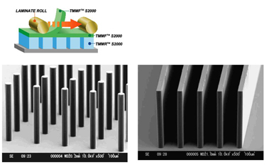
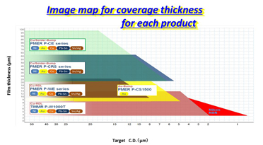
We have developed and commercialized optimal photoresists and processing equipment for a range of packaging processes, including the newest technologies. Photoresists for packaging are available for a wide range of production technologies including wafer-level CSP, SiP, RDL, TAB and COF. In the field of processing equipment, we have developed unique technologies for thick film processing, such as a coating machine that can form thick films at 20-100 μm with excellent CD uniformity.
MEMS manufacturing technology is widely used for the miniaturization and higher functionality of electronic components. This technology is an integrated combination of electricity, machinery, light and materials, and expected to be an integral part of fundamental technologies necessary for the development of electronic components. In fact, it has already been employed by some electronic components and introduced to manufacturing technologies of image sensors, inkjet nozzles, and high-frequency wave devices.
We have commercialized thick-film permanent photoresists for MEMS, and developed a non-spin coater that can form thick films capable of highly uniform photoresist coating at a 100 μm level with a single application and a developing machine for thick films. We offer high quality, most advanced and most effective processing technologies in the MEMS field as well, thus widely supporting the miniaturization of electronic components in terms of both materials and equipment.
Auxiliary Chemicals
- Strippers
Name of Products Usage Features Stripper - 10 Exclusive for positive. Water-soluble non-chlorine group solvent type / No corrosion to Al substrates. Stripper - 104 Exclusive for positive. Water-soluble non-chlorine group solvent type / No corrosion to Al substrates. Stripper - 105 / 106 Exclusive for positive. Water-soluble non-chlorine group solvent / Highly efficient type. SST-A2 / SST-A47 Exclusive for positive. Water-soluble non chlorine group solvent / Super high efficient type. (Al substrate) Stripper 502A /710 For both negative / positive Non-chlorine group solvent / Standard type. Clean Strip HP / HP-2 / MF For both negative / positive Non-chlorine group solvent / Non-phenol type. USR-100 Si-ARC Remover / positive Alkali Aqueous type ST-120 / ST-121 Wafer Level Packaging & TSV Cleaners / Both positive and negative Organic alkali / Made in USA - Developers
Name of Products Usage Features NMD-3 (2,38%, 25%)(Made in USA) Exclusive for positive Standard type / Metal free. Can develop different mix ratios as needed NMD-W (Made in USA) Exclusive for positive Surfactant type / Metal free. - Thinners
Name of Products Usage Features iLA Thinner (Made in USA) For both negative and positive photoresists. For removing photoresists at wafer edge, back-side and coater cup. Good solubility for all resists OK73 Thinner For both negative and positive photoresists. For removing photoresists at wafer edge, back-side and coater cup. Good solubility for all resists VFR Thinner For both negative and positive photoresists. For removing photoresists at wafer edge, back-side and coater cup. Standard Type ONNR-20 Thinner These chemicals are available for not only the semiconductor industry but also any other industry outside of semiconductor as well. Please let us know if you are looking for any of these products for your project regardless of industry. High quality Cyclohexanone (C6H10O) PM Thinner These chemicals are available for not only the semiconductor industry but also any other industry outside of semiconductor as well. Please let us know if you are looking for any of these products for your project regardless of industry. High quality Propylene Glycol Monomethyl Ether Acetate (C6H12O3) HP Thinner These chemicals are available for not only the semiconductor industry but also any other industry outside of semiconductor as well. Please let us know if you are looking for any of these products for your project regardless of industry. High quality 2-heptanone (C7H14O) EL Thinner These chemicals are available for not only the semiconductor industry but also any other industry outside of semiconductor as well. Please let us know if you are looking for any of these products for your project regardless of industry. High quality Ethyl lactate (C5H10O3)